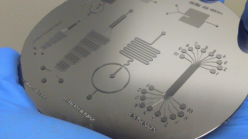
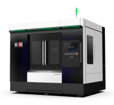
Microfluidic chip, as a technology platform to manipulate fluids in micron-scale space, has shown great potential for application in biomedicine, chemical analysis, environmental monitoring and other fields. The manufacturing quality and precision of microfluidic chip moulds directly determine the performance and application effect of microfluidic chips. Traditional manufacturing methods such as photolithography and etching have certain limitations in the face of complex structures and high precision requirements. The emergence of femtosecond laser technology has brought a new breakthrough in the manufacturing of microfluidic chip moulds.

I. Features and advantages of femtosecond laser
Femtosecond laser is a kind of ultrashort pulse laser with pulse width on the order of femtosecond (10^-15 seconds). It has the following significant features and advantages:
1. extremely high peak power: it can instantly achieve material removal and modification, avoiding the heat accumulation and heat diffusion problems in long-pulse laser processing.
2. ultra-fine processing capability: sub-micron or even nano-scale processing accuracy can be achieved to meet the high-precision requirements of microfluidic chip moulds for tiny structures.
3. non-contact processing: no mechanical pressure on the material surface, avoiding deformation and damage to the mould.
4. Multiple materials can be processed: both hard materials such as metal, ceramics, and soft materials such as polymers can be processed effectively.
5. Three-dimensional processing capability: able to manufacture microfluidic chip moulds with complex three-dimensional structure, expanding the function and application range of microfluidic chips.
Second, the principle of femtosecond laser manufacturing microfluidic chip moulds
The process of femtosecond laser interaction with materials mainly includes multiphoton absorption, avalanche ionisation and plasma formation. When the femtosecond laser focuses on the inside of the material, the extremely high peak power makes the material ionised in an instant, forming a plasma. The impact force generated by the rapid expansion of the plasma removes the material, thus realising the processing of microstructure.
III. Process Flow
1. Design the mould structure: according to the application requirements of microfluidic chips, use professional software to design the three-dimensional structure of the mould, including channel shape, size and layout.
2. Preparation of substrate material: choose suitable substrate material, such as silicon wafer, glass, metal or polymer, etc., and carry out surface cleaning and pre-treatment on it to improve the effect and quality of laser processing.
3. femtosecond laser processing: fix the substrate material on the high-precision motion platform, and realise the point-by-point scanning processing of the substrate material by controlling the parameters of the laser (pulse energy, pulse width, repetition frequency, etc.) and the trajectory of the motion platform to form the microfluidic channels and structures.
4. Quality Inspection: The dimensional accuracy, surface roughness and structural integrity of the moulds are inspected and evaluated using optical microscopes, scanning electron microscopes, atomic force microscopes and other equipment.

IV. Practical application cases
1. Polymer microfluidic chip mould manufacturing
- Researchers have successfully fabricated microfluidic chip moulds with complex three-dimensional channel structures on polymethylmethacrylate (PMMA) materials using femtosecond lasers.
- The fabricated microfluidic chip moulds were used for cell culture and drug screening experiments, and showed good biocompatibility and fluid manipulation performance.
2. Glass microfluidic chip mould fabrication
- Femtosecond lasers have processed microfluidic channels with high depth-to-width ratios on glass materials, with channel depths up to several hundred microns and aspect ratios exceeding 10:1.
- These glass microfluidic chip moulds are used for chemical analysis and microreaction experiments and have good chemical resistance and optical transparency.
3. Metal microfluidic chip mould fabrication
- Microfluidic chip moulds with high precision and surface quality have been fabricated on stainless steel for rapid mixing and separation of microfluidic experiments.
- The high strength and good thermal conductivity of metal moulds can provide more stable and efficient conditions for microfluidic experiments.
Femtosecond laser fabrication of microfluidic chip mould technology has a broad development prospect and application potential. Through continuous technological innovation and optimisation, it will provide stronger support for the development of microfluidic chip technology and promote its wide application and innovation in the fields of biomedicine and chemical analysis.
As an advanced manufacturing technology, femtosecond laser brings brand-new possibilities for the manufacturing of microfluidic chip moulds. Its advantages of high precision, non-contact and three-dimensional processing capability make the manufacture of complex, high-performance microfluidic chip moulds a reality. With the continuous progress and improvement of the technology, the application of femtosecond laser manufacturing technology in the field of microfluidics will continue to expand and deepen, bringing more opportunities and breakthroughs for the development of related fields.

