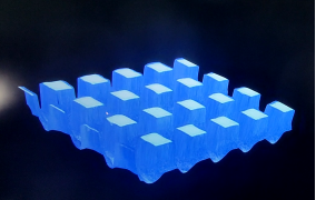
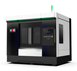
Femtosecond laser etching of bump microstructures is an advanced micro and nanofabrication technology with the advantages of high precision, high resolution and non-contact processing. The following is a detailed introduction about femtosecond laser etching bump microstructure:
I. Technical Principle
Femtosecond laser is a kind of ultrashort pulse laser, whose pulse width is extremely short, usually on the order of femtosecond (10-¹⁵ seconds). When the femtosecond laser is focussed on the surface of a material, due to its extremely high peak power and short pulse duration, it can produce extremely high energy density in an instant, causing a variety of physical and chemical changes in the material.
During the etching of the bump microstructure, the energy of the femtosecond laser is absorbed by the material, resulting in localised heating, melting and evaporation of the material surface. By precisely controlling the laser parameters (e.g. pulse energy, pulse width, repetition frequency, etc.) and scanning path, bump microstructures of various shapes and sizes can be etched on the material surface.
II. Fields of application
1. Microelectronics field:
- In integrated circuit manufacturing, femtosecond laser etching of bumped microstructures can be used to fabricate microelectrodes, bumped microstructure interconnects and three-dimensional packages. For example, by etching tiny bump microstructures on the chip surface, it can achieve high-density interconnections between the chip and external circuits and improve the performance and reliability of integrated circuits.
- It can also be used to fabricate microelectromechanical systems (MEMS) devices such as accelerometers, gyroscopes, and pressure sensors. By etching bump microstructures on the surface of MEMS devices, the sensitivity and response speed of the devices can be improved.
2. Optics:
- Femtosecond laser-etched bump microstructures can be used to fabricate diffractive optical elements, microlens arrays, and optical waveguides. For example, by etching periodic bump microstructures on the surface of optical materials, diffraction gratings can be fabricated for spectroscopy, filtering and optical imaging.
- It can also be used to make micro and nano-optical devices such as micro lasers, optical sensors and photonic crystals. By etching bump microstructures on the surface of optical materials, the optical properties of the materials can be changed to achieve the modulation and transmission of light.
3. Biomedical field:
- In the biomedical field, femtosecond laser etching of bump microstructures can be used to make biochips, microfluidic chips and tissue engineering scaffolds. For example, by etching tiny bump microstructures on the surface of biochips, the capture, separation and detection of biomolecules can be realised, and the sensitivity and accuracy of biological analysis can be improved.
- It can also be used to make tissue engineering scaffolds. By etching bump microstructures on the surface of the scaffolds, the attachment and growth of cells can be increased, and tissue regeneration and repair can be promoted.

III. Technical advantages
1. High precision and high resolution: the pulse width of femtosecond laser is extremely short, which can produce extremely high energy density in an instant and make the material undergo tiny changes. Therefore, femtosecond laser etching of bump microstructures can achieve high-precision and high-resolution processing, and the size of the etched bump microstructures can reach the nanometer scale.
2. Non-contact processing: Femtosecond laser etching of bump microstructures is a non-contact processing technology that does not cause mechanical damage to the material surface. Therefore, this technique can be used to process a variety of fragile and sensitive materials, such as semiconductor materials, optical materials and biological materials.
3. Flexibility and customisability: Femtosecond laser etching of bump microstructures allows flexible control of the shape, size and distribution of bump microstructures by precisely controlling the parameters and scanning path of the laser. Therefore, this technique can be customised to produce a variety of special bump microstructures according to different application requirements.
4. High efficiency and speed: Femtosecond laser etching of bump microstructures is a high-efficiency and high-speed processing technology that can etch a large number of bump microstructures in a short time. Therefore, this technology can meet the needs of mass production and rapid manufacturing.


